Water Treatment for Photolithography Rinse & Develop Processes
In semiconductor fabrication plants, the creation of integrated circuits depends on many sequential steps that require extreme precision and cleanliness. Photolithography is the pattern-transfer method that uses light to define microscopic structures on silicon wafers. After the photoresist has been exposed through a mask and chemically developed, the wafer is immersed in a series of ultrapure water rinses. The photolithography rinse and develop process is the carefully orchestrated post‑exposure sequence in which residual developer, dissolved solids and microscopic contaminants are removed before the wafer moves to etching. In plain English, the process is an advanced washing step that uses highly purified water to protect features that are often smaller than 20 nm. It stabilises the developed photoresist patterns, prevents capillary forces from collapsing delicate lines, and ensures that no ions or particles remain on the surface. Engineers pay close attention to the dynamics of fluid flow, surface tension and evaporation because each factor influences how well the patterns remain intact. In some fabs the rinse happens in semi‑automated spin‑rinse‑dry modules, while in immersion lithography the same ultrapure water serves as both immersion medium and rinse. Though simple in appearance, this process is a critical safeguard against lithography defects.
Beyond cleaning, post‑develop rinsing has significant business value for chip manufacturers. Defects introduced at the photolithography stage cascade through later steps and lead to yield loss, so preventing pattern collapse and bridging is central to profitability. Poor removal of developer can cause line width variation and footing; residual silica or metals may precipitate during drying and form bridges between lines. Even a few parts per billion of sodium or calcium can shift transistor threshold voltages, and organic residues can act as nucleation points for voids. To manage these risks, modern lines install multi‑stage ultra‑pure water (UPW) treatment, point‑of‑use ultrafilters and advanced monitoring. Water treatment intervenes at three points: it produces ultra‑low ionic and particulate content water upstream; it removes dissolved gases that could form bubbles; and it provides final filtration immediately before the water contacts the wafer. The business case for these investments is strong because the cost of contamination is orders of magnitude higher than the incremental cost of achieving sub‑ppt purity. As device dimensions shrink to 5 nm and below, the industry has adopted even tighter controls on silica, boron and organic compounds. Companies track defects by yield‑learning teams and correlate them with water‑quality excursions. Lessons learned from these analyses feed into capital planning for future plants, where water reuse and circularity are also considered. In this way, rinsing and developing is not just a technical step but a strategic element of semiconductor competitiveness.
Related Products for Photolithography Rinse & Develop
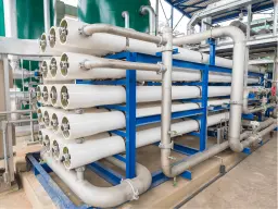
Reverse Osmosis
RO membranes are the primary barrier that removes over 99 % of dissolved salts, colloidal silica and organic molecules from feed water. They work by applying pressure to drive water through semi‑permeable membranes while rejecting ions and larger species. In the context of photolithography rinse lines, high‑rejection low‑pressure RO stages are often arranged in two passes to achieve permeate with conductivity below 1 µS/cm, which is then polished further.
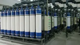
Ultrafiltration
UF modules with pore sizes between 0.01 µm and 0.1 µm remove colloidal particles, bacteria and endotoxins that earlier stages may not capture. In semiconductor applications, capillary UF membranes are sometimes operated in dead‑end mode to achieve particle counts below 200 per liter for particles larger than 0.05 µm. They also help retain sub‑micron silica polymers that can cause haze defects.
Electrodeionization (EDI)
EDI combines ion exchange resins with an electrical field to continuously remove trace ions without the need for chemical regeneration. After RO, EDI units polish the water to achieve resistivities approaching 18 MΩ·cm. Because they regenerate resins electrochemically, they minimise downtime and chemical waste. In rinse systems they provide stable ionic control and reduce the risk of silica breakthrough from exhausted resins.
Deionization
In some plants, mixed‑bed resin polishers remain as a back‑up to EDI or as a final stage. These polishers use strong‑base and strong‑acid resins in one vessel to scavenge remaining ions, achieving resistivity above 18.2 MΩ·cm. Because they are sensitive to exhaustion, silica breakthrough is monitored closely; when silica rises to a specified limit, the bed is regenerated or swapped.
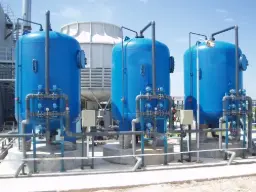
These systems are integrated in series to progressively remove different classes of contaminants and to provide redundancy. Reverse osmosis and EDI form the backbone of ionic control, while ultrafiltration and microfilters address particles and bacteria. UV oxidation and degasification protect against organic carbon and dissolved gases, which can influence photoresist chemistry and drying behaviour. Point‑of‑use filters ensure that any contamination introduced in distribution piping is removed just before contact with wafers, an essential safeguard because even cleanroom‑grade pipes can shed particles over time. Degasification contactors are particularly critical for immersion photolithography, where dissolved gas bubbles can refract light and distort patterns. Without this multistage treatment, the high volumes of rinse water required for sub‑10 nm patterning would present unacceptable risk to yield.
Key Water‑Quality Parameters Monitored
Engineers monitor a suite of water‑quality parameters to ensure that rinse water does not introduce defects. Electrical resistivity, measured at 25 °C, is a primary indicator of ionic purity. Typical values for semiconductor rinse water fall between 17.5 and 18.2 MΩ·cm. A resistivity drop often signals breakthrough of silica or boron from a resin bed or accidental contamination from metallic piping. Total Organic Carbon (TOC) is tracked with online UV persulfate analyzers; concentrations are kept below 1 µg/L to prevent organic film formation and micro‑bubbles during spin drying. Dissolved oxygen is measured continuously using optical sensors; levels between 1 µg/L and 10 µg/L are considered acceptable for photolithography, although immersion tools may specify even lower targets to avoid bubble nucleation. Particle counters using light‑scattering detection monitor counts of particles larger than 0.05 µm; high‑end fabs aim for less than 200 particles per liter. Metals and boron are analysed with inductively coupled plasma mass spectrometry (ICP‑MS) on grab samples; typical limits are below 1–10 ng/L because even trace metals can diffuse into silicon and alter electrical properties. Silica, both dissolved and colloidal, is monitored with colorimetric analysers; values below 50 ng/L are typical, and because silica is non‑conductive it can slip through resistivity monitoring unnoticed.
Water temperature and flow rate also influence rinse performance. Temperature is usually maintained between 20 °C and 30 °C to balance resist removal and evaporation rates; deviations can affect developer solubility and pattern critical dimensions. Flow rate controls the shear on the wafer surface and is adjusted so that boundary layers do not allow redeposition of contaminants. In spin‑rinse‑dryers, the water is delivered at high flow rates for a few seconds before spinning up to remove liquid. Microbial control is addressed by maintaining bacterial counts below 1 colony‑forming unit (CFU) per 100 mL; biofilms in distribution lines can shed endotoxins that cause pattern defects. pH measurement is not common in UPW because ionic content is so low, but operators ensure that carbon dioxide is stripped so that the apparent pH remains near neutral. Non‑volatile residue (NVR) measurements provide a gravimetric check on any residual solids left after water evaporation; typical values are below 100 ng/L. Instrument calibration is scheduled regularly because sensors drift at such low concentrations; conductivity and TOC sensors are calibrated monthly, while ICP‑MS calibrations occur weekly using traceable standards.
| Parameter | Typical Range | Control Method |
| Resistivity (25 °C) | 17.5–18.2 MΩ·cm | Two‑pass RO followed by EDI or mixed‑bed polisher; continuous conductivity monitoring |
| Total Organic Carbon (TOC) | < 1 µg/L | UV oxidation with 185/254 nm lamps, activated carbon pretreatment, online TOC analyzers |
| Dissolved Oxygen | 1–10 µg/L | Membrane degasifiers, nitrogen sweep gas, vacuum degassing |
| Particle Count ≥0.05 µm | < 200 particles/L | Ultrafiltration, microfiltration at point of use, periodic loop flushes |
| Silica (total) | < 50 ng/L | Anion exchange resins, monitored by colorimetric analyzers; regeneration triggered at 50 ng/L |
| Metals/Boron | < 1–10 ng/L | Mixed‑bed ion exchange, boron‑specific resins, ICP‑MS monitoring |
| Ions (anions and ammonium) | < 50 ng/L | Continuous EDI operation, anion/cation resin polishers |
| Bacteria | < 1 CFU/100 mL | Hot water sanitisation at 80 °C, UV disinfection, periodic chemical sanitisation |
| Non‑volatile residue (NVR) | < 100 ng/L | Polishing, final microfiltration, gravimetric testing |
| Temperature | 20–30 °C | Heat exchangers and chiller control loops |

Design & Implementation Considerations
Effective design of photolithography rinse water systems requires integrating engineering controls with cleanliness requirements. Loop architecture should minimise dead legs and stagnation to prevent microbial growth; distribution piping is typically constructed from high‑purity fluoropolymer materials such as PFA or PVDF to reduce leaching of metals and organics. Designing the loop as a closed recirculating system with constant velocity helps maintain an inert environment; velocities of 1 m/s or higher prevent particle settling. Elevating supply lines and draining points ensures that there are no trapped volumes where water can stagnate. Vibration‑isolated pumps with electropolished internal surfaces reduce particle generation. To support redundancy and maintenance, two parallel trains of RO and EDI with automatic isolation valves allow one train to be serviced while the other continues operation. Point‑of‑use filters are installed in easily accessible housings to facilitate quick changes without disturbing upstream cleanliness.
Standards provide a framework for system design. The SEMI F63 guide outlines performance criteria for semiconductor ultrapure water systems, including sampling points, instrumentation and quality targets. Designers also consider ISO 14644 cleanroom standards for air quality, because airborne particles can enter rinse baths when wafers are transferred. ASTM D5127 specifies reagent water types E‑1.3 through E‑1.6 for electronics, with E‑1.3B being the most stringent for photolithography; these types define acceptable ranges for resistivity, TOC and silica. Compliance with ISO 9001 or comparable quality management systems ensures that documentation, testing and traceability are rigorously maintained. Control strategies use programmable logic controllers (PLCs) and distributed control systems (DCS) to automate valve sequencing, flushing and alarms. Operators implement hazard and operability (HAZOP) studies to identify potential failure points, such as backflow from process tools or cross‑contamination from cleaning chemicals. Designing for waste minimisation is increasingly important; water reclaim systems recover rinse water for other less critical processes like back‑grinding or cooling, reducing overall consumption.
Material compatibility and footprint also influence implementation. Because photoresist developers often contain tetramethylammonium hydroxide (TMAH), the rinse system must be compatible with alkaline residues; this affects valve seals and pump materials. Selecting high‑purity gaskets and diaphragms prevents leaching of silicones and plasticisers. Space constraints inside fabs require compact modular treatment skids that can be prefabricated and craned into place. Acoustic and vibration isolation is critical in lithography areas because vibrations can distort optical alignments; pump skids are mounted on dampening pads and remote blowers may be located outside the cleanroom. Instrumentation is placed near points of interest but outside of process tool enclosures for easier maintenance; signals are transmitted via fibre‑optic or shielded cables to reduce electromagnetic interference. Implementation schedules must coordinate with fab construction and ramp‑up; commissioning of UPW systems often happens months before lithography tools are installed to allow for flushing, passivation and qualification. In high‑volume manufacturing, design also anticipates future capacity expansions by oversizing piping and leaving room for additional filtration stages.
Operation & Maintenance
Operating a rinse water system for photolithography requires vigilant monitoring and proactive maintenance. Operators track key parameters through a supervisory control and data acquisition (SCADA) system and respond to alarms immediately. Conductivity and TOC sensors provide continuous trends; if resistivity drops below 18 MΩ·cm, operators verify sensor calibration and then inspect mixed‑bed resins for exhaustion. Dissolved oxygen readings above 10 µg/L trigger checks on degasifier membrane integrity and sweep gas flow. Weekly calibration of conductivity, TOC and dissolved oxygen instruments ensures that readings remain accurate; reference solutions traceable to national standards are used. Pre‑filters upstream of RO units trap coarse particles; these cartridges are typically replaced monthly or when the differential pressure exceeds 0.2 bar. RO membrane performance is evaluated by calculating normalised permeate flow and salt rejection; cleaning in place (CIP) procedures are initiated when permeate flow drops by 10 % from baseline.
Maintenance intervals are based on operating hours and water quality. EDI modules are inspected for scaling and foulants every six months, though actual replacement occurs after several years if operated within design limits. UV lamps lose intensity over time; lamp replacement is scheduled annually or when on‑line sensors detect reduced photo‑oxidation efficiency. Ultrafiltration modules are back‑washed automatically using high‑purity water; a chemical cleaning with citric acid or sodium hypochlorite may be performed every quarter to recover permeability. Point‑of‑use filters in rinse tools are changed at intervals dictated by particle counts; some fabs replace them as often as weekly during sensitive production runs to prevent pattern bridging. Routine hot water sanitisation of distribution piping at 80 °C destroys biofilms and reduces microbial counts; this procedure may be conducted quarterly or after system modifications. Operators record every activity in a maintenance log for traceability and continuous improvement.
A typical calculation performed by operators is the reverse osmosis recovery, which uses the formula Recovery (%) = (Permeate Flow / Feed Flow) × 100. For example, if the feed flow is 50 L/min and the recovery setpoint is 80 %, the required permeate flow is 40 L/min. Meeting this target ensures membrane efficiency and influences downstream sizing. Operators also manage water hammer risks by programming valve openings and pump ramp‑ups to occur over several seconds rather than instantaneously. Inventory of consumables such as mixed‑bed resins, UV lamps and filter cartridges is tracked to avoid shortages. Training programs emphasise contamination control: technicians wear appropriate cleanroom garments, use dedicated tools for UPW systems and follow strict entry protocols. Through these operational practices, the rinse system consistently provides water of appropriate quality while minimising downtime and product risk.
Challenges & Solutions
Photolithography rinse systems face several recurring issues that can jeopardise yield. Problem: Breakthrough of silica or boron from exhausted ion exchange resins can occur suddenly, leading to a sharp increase in impurities that are not detected by resistivity meters. Solution: The implementation of silica‑specific online analyzers and the practice of replacing or regenerating resins based on cumulative throughput, rather than only resistivity, reduce this risk. Another Problem: Organic contaminants from upstream processes or from the degradation of polymeric pipes can cause haze on photoresist surfaces. Solution: Combining UV oxidation with downstream activated carbon and performing regular loop flushes helps maintain TOC levels below 1 µg/L and removes leachable organics before they reach the wafer.
Excessive microbial growth in distribution piping poses a different challenge. Problem: Even in high‑purity systems, biofilms can develop in dead legs or where velocities are low, releasing endotoxins that disrupt the photoresist layer. Solution: Designing loops without dead legs, maintaining velocities around 1 m/s, and conducting periodic hot water sanitisation at 80 °C are effective countermeasures. In immersion lithography, dissolved gas bubbles trapped between the lens and wafer can refract light. Problem: Inadequate degassing can leave dissolved oxygen above 10 µg/L, causing bubble formation and focal defects. Solution: Installing membrane degasifiers at both the main loop and at the point of use, and monitoring dissolved gas at the tool interface, ensures consistent low oxygen levels. Finally, changes in feed water quality due to municipal source variations can stress upstream treatment. Problem: Spikes in colloidal silica or organics reduce RO performance and accelerate fouling. Solution: Monitoring raw water and temporarily adjusting pretreatment chemistry—such as adding coagulation or microfiltration—maintains feed quality within design parameters and protects downstream membranes.
Advantages & Disadvantages
A controlled photolithography rinse and develop system offers significant benefits for semiconductor manufacturing, yet it also involves trade‑offs. On the plus side, high‑purity water rinsing drastically reduces defectivity. Stable resistivity, low silica and low organic levels translate into higher process yields and tighter line widths on the wafer. Efficient removal of developer and prevention of pattern collapse enable more aggressive geometries, supporting advanced nodes like 5 nm and 3 nm. Automated water systems reduce labour and variability; sensors provide real‑time data, allowing rapid response to anomalies. Integrated design with parallel trains improves system availability and allows maintenance without production downtime. There are environmental advantages too: modern systems incorporate water reclaim and reuse strategies, saving millions of litres of water per year and lowering the plant’s footprint. These features collectively contribute to operational excellence and competitive advantage in the electronics sector.
However, the disadvantages must also be acknowledged. The capital cost of ultra‑pure water systems is high due to the need for multiple treatment stages, high‑grade materials and sophisticated monitoring. Operating costs include energy for pumps and UV lamps, consumables like resins and filters, and periodic chemical cleaning. Complexity increases the maintenance burden; skilled technicians are required to operate and troubleshoot the system, and instrumentation calibrations are frequent. If not designed properly, the system can waste significant volumes of water through flushing and low recovery rates. Over‑reliance on sensors can lead to complacency; some contaminants such as colloidal silica are not detected by conductivity and require additional testing. Finally, expansion or upgrades can be challenging in tight cleanroom spaces, sometimes requiring downtime that impacts production schedules.
| Aspect | Pros | Cons |
| Water Quality | Extremely low ionic and particulate levels improve yield | Achieving sub‑ppt levels requires sophisticated systems |
| Productivity | Automated rinsing supports advanced nodes and reduces operator variability | Complex systems demand skilled staff and frequent maintenance |
| Environmental Impact | Water reclaim reduces consumption and supports sustainability | Energy consumption and waste streams add to operating cost |
| Flexibility | Modular systems allow maintenance and upgrades without full shutdown | Retrofitting in existing fabs can be space‑constrained and costly |
| Monitoring & Control | Continuous sensors enable quick response to deviations | Sensors may not detect all contaminants; reliance can be risky |
Frequently Asked Questions
Question: What makes rinse water quality so critical in photolithography?
Answer: The features patterned on semiconductor wafers are often smaller than the wavelength of visible light, so even minuscule contaminants can cause bridging or deformation of lines. Rinse water directly contacts photoresist patterns and must not introduce ionic, organic or particulate impurities. Poor water quality can lead to pattern collapse during drying, metal contamination that alters transistor behaviour, or organic films that scatter light. Maintaining ultrapure standards ensures that the lithography process yields consistent, defect‑free circuits. Engineers therefore treat the rinse step as part of the lithographic exposure strategy rather than a simple cleaning operation.
Question: How does dissolved silica in rinse water affect photoresist patterns?
Answer: Silica, whether dissolved or colloidal, can precipitate onto wafer surfaces during spin drying. Since silica is electrically insulating and non‑conductive, it is not detected by simple conductivity sensors and can escape unnoticed. Deposited silica particles create bridges between adjacent lines or introduce defects known as “haze”, which reduce optical clarity and lead to yield loss. To mitigate this, semiconductor fabs use strong‑base anion exchange resins to remove silica and employ colourimetric silica analysers to trigger resin change‑out before breakthrough. Keeping total silica below 50 ng/L has proven effective for sub‑20 nm patterning.
Question: Why are UV oxidation and degasification combined in rinse water systems?
Answer: UV oxidation uses high‑energy photons to convert dissolved organic compounds into carbon dioxide and water. The process also produces dissolved gases like carbon dioxide and oxygen as byproducts. Degasification, using membrane contactors or vacuum stripping, removes these gases along with residual oxygen from upstream processes. Without degasification, dissolved gases can form micro‑bubbles during spin drying or immersion, causing streaks and distortion. Combining UV oxidation with degasification ensures that TOC levels stay below 1 µg/L while dissolved gas concentrations remain low, thereby preventing both organic scumming and bubble defects.
Question: How often should point‑of‑use filters be replaced?
Answer: Replacement frequency depends on the production environment, wafer throughput and sensitivity of the devices being manufactured. In high‑volume manufacturing for advanced nodes, point‑of‑use filters may be changed as often as every week to maintain particle counts below 200 per litre. Operators monitor differential pressure and particle counts downstream of the filters; when either rises above setpoints, the filter is replaced. Scheduled replacement during preventive maintenance is often aligned with tool maintenance windows to minimise downtime. Keeping spare filters on hand is essential to avoid interruptions.
Question: Can rinse water systems be designed for sustainability without compromising quality?
Answer: Yes, many modern fabs incorporate water reuse and resource‑efficient designs. Rinse water from high‑purity steps can be captured, monitored and reused in less critical processes like back‑grinding or cooling towers. High‑recovery RO membranes and staged filtration reduce the volume of reject water. Energy‑efficient pumps and LED‑based UV lamps lower power consumption. Automation allows precise control of flushing sequences, minimising water waste. While ensuring water purity always takes precedence, thoughtful engineering can balance sustainability with stringent quality requirements.